Tutorials

TUTORIAL #1
Machine Learning for Design Automation
The widespread usage of machine learning and deep learning has fundamentally reshaped the information infrastructure and human society. It also brings new opportunities for design automation of VLSI. With machine learning techniques, labor intensive and time-consuming IC design cycles can be accelerated effectively. This tutorial will present recent research progress on machine learning for various stage in design automation, especially on high level synthesis, timing analysis, thermal modeling and yield analysis.
| Organizer: | Prof. Yuanqing Cheng, Beihang University, Beijing, China. |
| Participants: | Prof. Wei W. Xing, Sheffield University, Sheffield, UK. |
| Prof. Kang Zhao, Beijing University of Telecommunications, Beijing China |
Talk 1: Heuristic Method for High-level Synthesis
With the increasing speed of chip design iteration, high-level synthesis (HLS) technology is considered an effective shortcut to achieve agile design and development. HLS mainly automatically converts C/C++high-level descriptions into appropriate hardware RTL descriptions, and performs prototype verification on FPGA. The report will introduce high-level integrated processes and key compilation scheduling techniques. From the perspective of the academic community, analyze the difficulties and challenges which can be solved using heuristic algorithms.
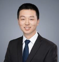
Dr. Kang Zhao is the professor of the Beijing University of Posts and Telecommunications (BUPT). He has been deeply involved in the field of integrated circuit EDA for nearly 20 years, and has both college work experience and rich experience in high-end product design of international leading enterprises. In 2009, he got the doctoral degree from Tsinghua University, and then continued to work in Tsinghua for 2 years. Then he worked in Intel, Xilinx and AMD for 12 years. In 2022, he came back to academic. The research focus is mainly on the EDA and FPGA, especially high-level synthesis. When Kang was in Xilinx, he played as a very important role and lead the HLS product team. Except for HLS, he also focused on AIE acceleration, heterogeneous computing, placement and routing.
Talk 2: Machine Learning for Thermal Modeling and Timing
As the integration density on-chip increases quickly with technology node shrinking, thermal dissipation becomes a severe problem for high performance chip design. Although traditional analytical models can capture on-chip thermal profile accurately, they are usually very time-consuming, and difficult to be integrated with iterative physical design phase. So in the first part of this talk, I will introduce recent research progress on using machine learning for thermal modeling such that the thermal aware physical design can be effectively accelerated and the hotspot can be captured as early as possible to mitigate thermal issues before sign-off stage. In addition, today’s billion scale chip design makes timing closure a challenging task due to sharply increase of process corners. In the second part of this talk, I will present how to take advantage of machine learning to accelerate timing analysis for deep sub-micron VLSI design.
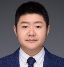
Yuanqing Cheng (S 11, M 13, SM 21) received the Ph.D. degree from Institute of Computing Technology, Chinese Academy of Sciences, Beijing, China, in 2012. During 2012 2013, he worked as a post doc researcher in LIRMM, CNRS, France. He is now a tenured associate professor of Beihang University, Beijing. His research interests include reliable and physical design for 3 D integrated circuits, reliable, and low power design for emerging technologies, such as spintronics and carbon nanotube technologies. He has pu b lished more than 50 peer review papers including Proc. of the IEEE, DAC , ICCAD, TVLSI, TCAD, etc. He is an IEEE senior member and the secretary of IEEE CEDA Beijing Chapter.
Talk 3: AI Powered Sampling Methods for Yield Analysis and Optimization
Yield estimation and optimization are two fundamental problems in back end electronic design automation (EDA), particular with the latest technology nodes. In this tutorial, we will introduce how the latest AI method can boost up the yield analysis and optimization with significant speedup and accuracy improvement. From the perspective of the academic community, outline the difficulties and challenges which can be solved using modern AI methods.
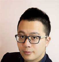
Dr. Xing Wei is a lecturer at the University of Sheffield, UK. He earned his Doctorate in the University of Warwick, UK, in March 2017. Dr. Xing specializes in intelligent manufacturing and the industrial application of artificial intelligence, with a notable focus on Electronic Design Automation (EDA). Throughout his career, Dr. Wei has published an impressive array of 50 academic papers in prestigious journals such as Appl. Math. Model. and J. Comput. Phys. He has also made significant contributions to top tier conferences in the realms of artificial intelligence (AAAI, NeurIPS, IJCAI) and EDA (DAC, ICCAD). Dr. Xing’s achievements in yield optimization were highlighted by his nomination for the Best Paper at ICCAD 2023. Additionally, his work in medical image processing was recognized with the Best Academic Poster Award at the IPMI 2019 conference. His research in digital twins won the Beijing Science and Technology Progress Award in 2023.
TUTORIAL #2
Exploring Radiation Effects for Reconfigurable SoCs
in Space and Particle Accelerators
The tutorial provides an in-depth overview of electronic failures induced by radiation in radioactive environments, such as space and particle accelerators. The first part delves into the radiation effects, considering the radiation environment of the Large Hadron Collider (LHC) at CERN, emphasizing comparisons with atmospheric conditions. The second part focuses on the reliability analysis of Reconfigurable Systems-on-Chip, discussing challenges and methodologies for evaluating radiation-induced effects on these systems.
| Organizers: | Dr. Corrado De Sio, Politecnico di Torino, IT |
| Dr. Matteo Cecchetto, CERN | |
| Dr. Rubén García Alía, CERN |
Talk 1: Electronic Failures in the Accelerator Radiation Environment and Test Facilities
The talk introduces the radiation-induced effects in electronics, with a particular focus on the radiation environment in the Large Hadron Collider (LHC) accelerator at CERN, presenting several comparisons with the atmospheric environment. It shows how the radiation levels are measured and simulated in critical areas of the accelerator, focusing on thermal and higher energy neutrons, which are one of the main threats for SEEs. Indeed, SEEs induced by thermal, and 0.01-10 MeV neutrons can induce more failures than high energy neutrons in several locations of the accelerator, and the related Radiation hardness Assurance (RHA) implications are presented. Finally, an overview of the test facilities employed at CERN to measure and qualify electronics is outlined.

MATTEO CECCHETTO received a master’s degree in electronic engineering from the University of Padova (Italy) in 2017 and performed a PhD at CERN (Switzerland), obtaining the degree from the University of Montpellier (France) in 2021. He is currently working on the Radiation to Electronics (R2E) project at CERN. His main activities focus on the experimental and Monte Carlo simulation study of neutron-induced single-event effects in accelerator and fusion environments, with a focus on the effects of thermal and intermediate-energy neutrons and related implications on the qualification approach for electronics.
Talk 2: Reliability Analysis for Reconfigurable Systems-on-Chip
Thanks to their performance, reduced power consumption, and adaptability, Reconfigurable Systems-on-Chip has emerged as a cutting-edge platform for many performance-oriented applications. Additional efforts are needed to ensure the correct system functionality for applications where reliability is a primary concern. Radiation environments are particularly challenging due to the high sensitivity of SRAM-based reconfigurable systems to single-event effects. The tutorial focuses on motivation, challenges, and methodology for evaluating radiation-induced effects on Reconfigurable Systems-on-Chip.

CORRADO DE SIO received the M.S. degrees in Computer Engineering from the University of Pisa, Pisa, Italy, in 2018. He received his Ph.D. from Politecnico di Torino, Turin, Italy, in 2023. Currently, He is working in the CAD & Reliability group of the Department of Computer and Control Engineering of Politecnico di Torino as a Postdoctoral Research Assistant and member of the Aerospace, Safety and Computing (ASaC) Lab. His research interests include reconfigurable devices, radiation effects, and EDA tools for analyzing and improving the reliability and the design of embedded and reconfigurable systems applications.
TUTORIAL #3
Integrating Multiple Knowledge-based Automation Methodologies
into the A/MS IC Design Flow
In the rapidly evolving field of integrated circuit (IC) design, the quest for efficiency, miniaturization, and power optimization has led to the development of innovative methodologies that promise to redefine traditional design flows. This tutorial presents a holistic approach to analog/mixed-signal IC design, focusing on the integration of cutting-edge techniques such as the gm/ID method for transistor sizing, Expert Design Plan (EDP) for procedural design automation in combination with ML characterization, Intelligent IP (IIP) for technology-agnostic schematic and layout generation, and SWARM for autonomous layout optimization. Aimed at both industry professionals and academic researchers, this tutorial will provide a deep dive into each method, showcasing how they can be synergistically applied in the future to streamline the design process, enhance design quality, and accelerate the development of ultra-low power (ULP) sensors and analog/mixed-signal (A/MS) circuits.
| Organizers: | Dr. Benjamin Prautsch, Fraunhofer IIS/EAS, DE |
| Prof. Ralf Sommer, TU Ilmenau, DE | |
| Prof. Jürgen Scheible, Reutlingen University, DE | |
| Participants: | Uwe Eichler, Fraunhofer IIS/EAS, DE |
| Lorenz Renner, TU Ilmenau, DE | |
| Yannick Uhlmann, Reutlingen University, DE | |
| Till Moldenhauer, Reutlingen University, DE |
Talk 1: gm/ID and Machine Learning Sizing
The presentation introduces the gm/ID method, an advanced technique for efficiently sizing transistors based on their operating points. Unlike traditional approaches such as the Square-Law method, the gm/ID method utilizes characteristic curves or lookup tables derived from a multidimensional DC analysis of the SPICE transistor model. This allows for accurate transistor sizing without the need for post-simulation adjustments, as the sizes are directly derived from the characteristic curves.
The second part focuses on the innovative use of neural networks (NNs) for transistor sizing using the gm/ID method. Neural networks learn from existing lookup tables and capture complex relationships to enhance accuracy without requiring extensive storage. This technique allows design strategies to be expressed in terms of electrical characteristics, reducing dependence on geometric quantities and process design kits (PDKs) and enabling efficient sampling and characterization of entire circuits.

Ralf Sommer's academic journey began at the Technical University of Braunschweig from 1983 to 1988 where he studied Electrical Engineering. His research culminated in 1993 with a PhD, the thesis being "Concepts and Procedures for Computer-Aided Design of Analog Circuits". He then joined the University of Kaiserslautern and the Fraunhofer Institute for Industrial Mathematics (ITWM) from 1993 to 2000. His role involved spearheading the project "Computer-Aided Design of Analog Circuits" along with the development of the symbolic analysis tool "Analog Insydes". He transitioned into the corporate sector in 2000, joining Infineon Technologies AG, Munich. He served as the Group Leader for "Analog Simulation" and shared responsibility for the research complex "Design Automation" in central CAD. Since 2006, Ralf Sommer has been holding a joint position at the Technical University of Ilmenau and at the Institute for Microelectronics and Mechatronics Systems GmbH (IMMS). He serves as professor for "Electronic Circuits and Systems" at TU Ilmenau, and as the scientific managing director of IMMS.

Lorenz Renner studied Electrical Engineering at the Ilmenau University of Technology. Since his graduation in 2023, he has worked as an analog IC design engineer at the microelectronics department of the Institute for Microelectronics and Mechatronics Systems GmbH (IMMS) in Erfurt. He aims for a PhD in the field of analog IC design and EDA, supervised by Professor Ralf Sommer at the Ilmenau University of Technology.

Yannick Uhlmann received his B.Eng. in Computer Engineering from Esslingen University in 2015, and his M.Sc. degree in Power and Microelectronics from Reutlingen University in 2017. Since 2018, he is a research assistant in Professor Scheible's EDA research group at Electronics & Drives, where he is pursuing a PhD with a focus on machine learning based analog IC design automation methods.
Talk 2: EDP for Circuit Design
In the second block of the tutorial, the Expert Design Plan (EDP) is discussed. EDP is an approach that encapsulates the knowledge and methodology of experienced analog designers in a reusable script. EDP enables designers to automate the entire design process from topology creation to final sizing using a special language (EDPL) and a comprehensive toolset. This includes functions for drawing circuit diagrams, setting up and executing simulations, evaluating simulation results, and exploring the design space. Previous EDP applications show that a bandgap reference circuit can be designed in less than 15 minutes and the analog parts of a 10-bit SAR-ADC fully automatically in about 100 minutes. In the talk the user interface and usage of EDP for a simple design task is demonstrated

Jürgen Scheible studied Electrical Engineering at the Technical University of Karlsruhe, where he received a PhD in 1991 with a thesis in the field of Electronic Design Automation. In 1992 he joined the „Automotive Electronics“ division of Bosch, the world's largest automotive supplier, where he held various roles. At Bosch he worked as Senior Engineer in ASIC design and as Project Manager for Bosch‘s layout design flows. As a Group Leader he was responsible for Bosch’s IC design environment, and he headed the IC layout design department for seven years. Since 2010, he is a Full Professor for Electronic Design Automation at Reutlingen University. Until 2023 he headed the master course "Power- and Mikroelectronics" there and was spokesperson for the "Electronics & Drives" Lab. His research interests include knowledge-based and AI-supported methods for the automation of analog IC circuit and layout design. In 2020, he published a textbook for layout design of electronic circuits. In 2023, he received the "EDA Achievement Award" from edacentrum, Hanover, a European academic and industrial network for electronic design and applications.
Talk 3: Layout: SWARM & Intelligent IP
The third part of the tutorial focuses on innovative A/MS layout methodologies. The two specific methods SWARM and Intelligent IP (IIP) will be presented. SWARM uses a decentralized approach with both formalized and non-formalized knowledge where self-organizing modules autonomously develop an optimal layout for given constraints. This methods leads to compact and efficient chip layouts. IIP employs generator-based and template-based methods such that it enables technology-independent description and automation of schematics and layouts. It facilitates the transfer of designs between different manufacturing processes while preserving design integrity. The talks emphasize the advantages of these methods in terms of layout creation speed, high usability with low initial efforts, as well as flow integration that will help design engineers in product development

Benjamin Prautsch received the Diploma degree (Dipl.-Ing.) and the doctoral degree (Dr.-Ing.) in electrical engineering from the Dresden University of Technology in 2013 and 2022, respectively. Since 2013 he is with Fraunhofer IIS/EAS and since 2018 he is heading the group Advanced Mixed-Signal Automation. Benjamin is responsible for generator-based analog design automation and reuse-oriented methods for new design flows. He and his team have been developing these topics in various national and European projects as well as in industrial R&D projects.
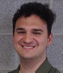
Till Moldenhauer earned his Bachelor's degree in Electrical Engineering from DHBW Stuttgart in 2019, followed by his Master's degree in Power and Microelectronics from Reutlingen University in 2023. From 2019 to 2023, he worked as a research and development engineer at Andreas Stihl AG & Co. KG in the electronics for robotic lawn mowers department. Since 2023, he has been pursuing a PhD at Reutlingen University, specializing in electronic design automation, with a focus on algorithms for physical design automation.
Uwe Eichler received the Dipl.-Ing. degree in Electrical Engineering from the Dresden University of Technology, Germany, in 2002. Since then he is with Fraunhofer EAS. As a research assistant he was concerned with several projects in the areas system-level modeling and simulation, mixed-signal simulation software development, and digital and analog CAD support. Since 2010 he is significantly involved in the analog integrated circuit design automation activities and one of the key technology developers of the Intelligent IP analog generator approach
TUTORIAL #4
Tackling Signal Integrity Challenges in Interposer and 3DIC Applications with Ansys RaptorX
In the evolving landscape of heterogeneous integration, designers face multiphysics challenges in ensuring signal integrity on silicon interposers and 3DIC architectures. Co-extraction of the signals with the power and ground nets to account for all potential electromagnetic coupling is crucial. Ansys RaptorX offers a robust solution, ensuring secure and efficient sign-off by addressing these signal integrity challenges with its advanced modeling capabilities. In this tutorial, case studies will be presented to showcase the strength of the RaptorX modeling engine, followed by a live demonstration of the tool on an interposer design.
| Organizers: | Dr. Konstantis Daloukas, ANSYS, GR |
| George Drasidis, ANSYS, GR | |
| Georgia Krokou, ANSYS, GR | |
| Presenter: | Georgia Krokou, ANSYS, GR |

Georgia Krokou is a Lead Application Engineer at Ansys since February 2019. Before this, she was with Helic, where she worked as an Application Engineer from April 2016, and as a Software Engineer starting in October 2011. She holds a Diploma in Computer and Communication Engineering, and an MSc in Computer and Communication Science, both from the University of Thessaly.
